PEMTRON to Exhibit Inspection Solutions for Semiconductor and Advanced Packaging at SEMICON China 2026
PEMTRON, an inspection equipment developer and supplier, will exhibit its latest inspection and metrology systems at SEMICON China 2026, taking place March 25–27 at the Shanghai New International Expo Centre. The company will showcase inspection solutions designed to support yield improvement, early defect detection, and process control across semiconductor and advanced packaging production.
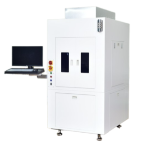
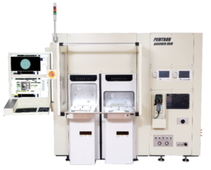 At the show, PEMTRON will showcase the 8800WIR Helios Wafer Inspection System, JUPITER 3D X-ray Inspection System, MARS Automated Visual Inspection (AVI) System, and the POSEIDON wafer measurement platform.
The 8800WIR Helios Wafer Inspection System combines advanced 2D and 3D imaging technologies to inspect a wide range of bump structures, including micro bumps. Designed for early-stage defect detection, the system helps identify quality issues before they impact subsequent manufacturing processes. By detecting small and difficult-to-find defects at the wafer level, 8800WIR supports improved yield and product consistency.
 The JUPITER 3D X-ray Inspection System provides both 3D and 2D inspection using PCT reconstruction-based processing. The system integrates high-resolution imaging with PEMTRON’s AOI defect detection algorithms to support in-line process monitoring and process analysis. JUPITER also enables data sharing with SPI and AOI systems, giving manufacturers clearer insight into process trends and production stability.
For memory module production, PEMTRON will feature the MARS Automated Visual Inspection (AVI) System. Designed for high-volume environments, MARS delivers fast, consistent inspection using advanced image processing to detect defects without compromising throughput or inspection accuracy.
PEMTRON will also present the POSEIDON system, which provides precise measurement of wafer warpage, flatness, and FC-BGA bump coplanarity—critical parameters for wire bonding, Micro LED, and advanced packaging processes. The system also captures fine surface defects such as microcracks, missing bumps, and bridging, supporting tighter process control early in production.
 SEMICON China attendees are invited to visit PEMTRON to learn how these inspection systems support reliable manufacturing across wafer-level, packaging, and memory applications.
For more information about PEMTRON, please visit www.pemtron.com.
About PEMTRON
Based on 3D precision measurement and vision source technology, PEMTRON develops equipment used in various fields such as SMT, Automotive Field, Lead Tab, Semiconductor, and supplies
 Soldering Inspection equipment (3D SPI), 3D Mounting Inspection equipment (3D AOI, MOI), Conformal Coating Inspection equipment (TROI-8800 CI), Bottom Head Inspection equipment (Eagle 8800TH), Top & Bottom Double Sided Simultaneous Inspection equipment (Eagle 8800TWIN), Automated X-Ray SMD Counter (MERCURY), Wafer Sawing Before/After 3D Inspection equipment (8800 WI/WIR), Wire Bonding 3D Inspection & MEMS Auto Inspection equipment(ZEUS), Package AVI equipment (APOLLON), Memory Module / SSD Auto Inspection equipment (MARS), FC-BGA, FCP-CSP Inspection equipment (POSEIDON-S), Scale Sorter Of FC-BGA Products (8800 FI), Bump Metal Mask Inspection equipment (8800 MI), PCB Appearance Inspection equipment (8800 AI) and Lead Tab Process/Inspection equipment(Hawk 7300).
